
Samsung Electronics has announced it has developed an all-DRAM stacked memory package using "through silicon via" (TSV) technology.
The new wafer-level-processed stacked package (WSP) consists of four 512Mb DDR2 chips that offer a combined 2Gb of high density memory. Using the TSV-processed 2Gb DRAMs, Samsung can create a 4GB DIMM.
In today's MCPs, memory chips are connected by wire bonding, requiring vertical and horizontal spacing between dies. By contrast, Samsung's WSP technology forms laser-cut micron-sized holes that penetrate the silicon vertically to connect the memory circuits directly with a copper filling, eliminating the need for gaps of extra space and wires protruding beyond the sides of the dies.
These advantages permit Samsung's WSP to offer a significantly smaller footprint and thinner package. Inside the new WSP, the TSV is housed within an aluminum (Al) pad to escape the performance-slow-down effect caused by the redistribution layer.
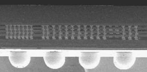
Chips are connected via "vias" instead of wire bonds
Photo: Company
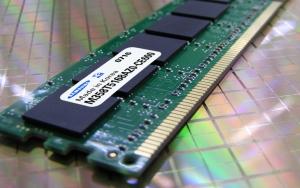
Samsung said it could now offer 4GB DIMM via its new TSV technology
Photo: Company

