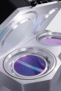
Applied Materials has unveiled a new chemical vapor deposition (CVD) technology capable of electrically isolating the densely-packed transistors in 20nm-and-below memory and logic designs with a high-quality dielectric film. The gaps between these transistors can have aspect ratios of more than 30:1 - five times higher than current requirements, the tool vendor claimed.
Using Applied's proprietary Eterna flowable CVD (FCVD) process, the system delivers a liquid-like film that flows freely into any structure shape to provide a bottom up, void-free fill, the vendor said.
Applied said its Eterna FCVD tools are being installed at six customer sites for DRAM, flash and logic applications.
"The need to fill smaller and deeper structures in advanced chip designs creates a physical roadblock for existing deposition technologies. Applied has broken through this barrier today with the introduction of its new Eterna FCVD system – delivering the disruptive technology that can enable the continued progress of Moore's Law," said Bill McClintock, VP and GM of Applied's DSM/ CMP business unit.

Applied Eterna FCVD system
Photo: Company


