

Being ubiquitous is the ultimate fantasy of mobile networking as it is the goal for users to be connected anywhere at anytime. One of the keys to achieve this is definitely the "ultra mobile" networking devices. To actualize the dream of being ubiquitous, IT hardware firms have been competing to make devices lighter and demanding components to be thinner and smaller to reduce the size of PCBs. It has been a great challenge for component makers to find ways to reduce the surface area while improving the functionality and durability of the products. Taiwan-based inductor maker Chilisin, in response to the trend of commercialization of mobile networking products, made an early start to develop thin and small-size inductors and improving yields. Now Chilisin has a full range of light and thin solutions to satisfy multiple needs of the light and slim mobile devices.
The smartphone, ultrabook and tablet markets are Chilisin'smajor focuses. The winning factor of Chilisin's inductorsin the ultra mobile device markets is their ability to provide higherperformance in a thinner and smaller form factor. For specific segments in the smartphone, ultrabook and tablet markets, Chilisin has introduced corresponding miniaturized components. These product lines can be divided into two major categories: miniaturized high frequency inductor components and miniaturized power inductorcomponents.
Slim form factors spurring demand for miniaturized inductors
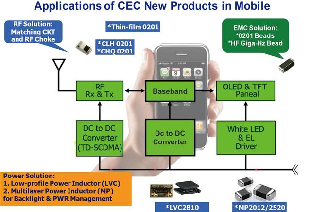
Chilisin has a range of products to suit the demand for high-frequency chip inductors such as 0402 and 0201 ferrite beads, 0201 ceramic chip inductors and 0201 thin-film inductors. As for miniaturized power inductors, Chilisin offers 0603 magnetic high-current beads, multilayer power inductors, molding power inductors and magnetic epoxy sealedwire-wound power inductors.
Chilisin emphasizes that there are certain technological barriers to shrink inductor components that need to be overcome. Take the printing of high SRF ferritebeadsfor example. Originally they had a surface area of 1.0x0.5mmbut now the printing must be done on a surface area of 0.5x0.5mm. Printing on such a small area requires more layers to keep the original DC resistance. Chilisin indicates that the dry process plays an important role in miniaturizing and thinning inductors. Chilisin began installation of dry process equipment in 2010, and therefore has taken the leadership role in the progress towards miniaturization.
With precise photo mask exposure during the thin-film process and superior circuit designs, Chilisin has been able to develop thin-film high-frequency inductors as small as size 0201. While their size is drastically smaller, the productsoffer multiple inductance values, tolerance of +/-0.1nH, high Q factor and low power loss at high frequency, which make them suitable for high-end smartphones, ultrabooks and tablets.
Product size shrinking raises the technological barriers
For power inductors, Chilisin's 0603 products have achieved highcurrent and lowDC resistance (DCR) requirements that previously only size 0805 was able to meet. Reducing the product's size by half while keeping the original rated current (IDC) and DCR value means putting the same amount of wiring into a smaller space. This requires superior designs and stable production processes to achieve. In addition, Chilisin has introduced multilayer power inductors made using internally developed powder materials that have allowed the company to shrink them to as small as 1.6x0.8mmwith a height as low as 0.5mm. To meet demand for high-current power applications, Chilisin supplies not only magnetic epoxy sealed power inductors with a height as low as 0.8mm, but also molding power inductors with a height as low as 1.0mm to satisfy the demand for thinner smartphones, ultrabooks and tablets.
The successful handset design-win strategy
With the life cycles of smartphones becoming shorter, Chilisin began to actively take part in high-end handsets' "design-win" process last year. This allows the firm to participate in handset chip designers' R&D process and modify products according to the designers' needs. This also allows the firm to avoid second-source price competition while pursuing technological improvements along with chip designers and in line with market trends. This type of transition relies on timely and superior R&D strength. Chilisin has already achieved significant results in the design-in market. It also has been receiving good reviews and trust from major handset makers and handset chip suppliers.
To better serve the need of US-based customers, Chilisin has set up a branch office in Silicon Valley, California to seamlessly cooperate with clients as early as the design stage without delay. This strategy has achieved huge success. Chilisin indicates that as of the end of March, the firm hadachieved on-year revenue growths for six months in a row. The first-quarter 2012 consolidated revenues showed an on-year growth of 16%. If the firm continues to perform stably in the second quarter, revenues are likely to grow steadily in the third quarter and even in the second half of 2012. Significant revenues can be expected for the entire year.
As for expansion in the market, Chilisin will actively participate in exhibitions to tap into new markets such as Russia and Japan. Chilisin looks to maintain its leadership in the inductor industry by extending its presence to more markets.
Chilisin's inductors satisfy the needs of ultra mobile smartphones
DIGITIMES' editorial team was not involved in the creation or production of this content. Companies looking to contribute commercial news or press releases are welcome to contact us.

