

Entegris, Inc., a leader in contamination control and materials handling technologies for highly demanding advanced manufacturing environments, and imec, a world-leading research center in nanoelectronics, announced they are collaborating to advance the development and broaden the adoption of 3D integrated circuits.
3D IC technology, a process by which multiple semiconductor dies are stacked into a single device, is aimed at increasing the functionality and performance of next-generation integrated circuits while reducing footprint and power consumption. It is a key technology to enable the next generation of portable electronics such as smartphones and tablets that require smaller ICs which consume less power.
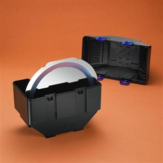
One of the key steps in 3D IC manufacturing process entails thinning semiconductor wafers while they are bonded to carrier substrates. Handling such thinned 3D IC wafers during the production process can result in wafer breakage, edge damage, and particle generation. A standardized, fully automated solution that supports the handling of multiple types of wafers would result in a significant cost reduction and pave the way toward further development and scaling of 3D IC technologies. Imec and Entegris are working on creating a solution to safely transfer and handle multiple kinds of 3D IC wafers without the risk of breakage and other damage that may occur during the 3D production process.
"We are excited to work with the imec team, which is a key research center leading technology innovation for the semiconductor industry," said Bertrand Loy, president and CEO of Entegris. "Our current collaboration is aimed at leveraging our wafer handling expertise and technology to reduce contamination and breakage by applying full automation to the handling of thin wafers during 3D wafer production. This project builds on our previously completed work with imec to develop dispense and filtration methods to reduce bubble and defect formation during the dispense of material that is used to temporarily bond 3D wafers to carrier substrates," said Loy.
"This collaboration with Entegris aims at developing a solution toward fully automated handling of multiple types of 3D IC wafers," stated Eric Beyne, Director of imec's 3D integration research program. "Such a general solution would imply a significant reduction of the development cost, which is key to the realization of a scalable and manufacturable 3D IC technology."
To learn more about Entegris' comprehensive suite of filtration and wafer handling solutions, see Entegris at booth 176 at SEMICON Taiwan, September 4-6, 2013. For more information, please contact Entegris at: asia_news@entegris.com. Join our SEMICON Taiwan event (http://on.fb.me/19ibAdQ) on Facebook to stay connected with the latest announcements before and during the show.
Learn more about imec's 3D integration research at the Tawain edition of the IMEC TECHNOLOGY FORUM, organized in conjunction with SEMICON Taiwan and in collaboration with SEMI on September 4, 2013 at the Taipei World Trade Center Nangang Exhibition Hall, Taipei, Taiwan. For more information: http://www.itf2013taiwan.be/
About Entegris
Entegris is a leading provider of a wide range of products for purifying, protecting and transporting critical materials used in processing and manufacturing in the semiconductor and other high-tech industries. Entegris is ISO 9001 certified and has manufacturing, customer service and/or research facilities in the United States, China, France, Germany, Israel, Japan, Malaysia, Singapore, South Korea and Taiwan. Additional information can be found at http://www.entegris.com/.
FFS_300mm_Open-300
DIGITIMES' editorial team was not involved in the creation or production of this content. Companies looking to contribute commercial news or press releases are welcome to contact us.

