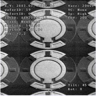
Malaysian based wafer foundry, SilTerra Malaysia Sdn. Bhd., today unveiled a "Piezoelectric Micromachined Ultrasound transducer (PMUT) on CMOS" platform for finger-print sensing and medical imaging applications.
This unique process platform offers a truly monolithic solution and integrates the PMUT on the top of the CMOS resulting in a single-chip solution. The PMUT is formed using a CMOS compatible piezoelectric material and surface micro-machining techniques.
Designers can choose any of the SilTerra's traditional CMOS/BCD/RF/Ultra low power platforms (180nm or 130nm) and build the PMUT on the top of these platforms.
This platform is supported by the relevant CMOS IP and PDK to enable a fully integrated System-On-Chip.
The PDK supports a configurable PMUT cell to address different end market applications such as a 20MHz PMUT cell for finger-print sensing or a 5MHz PMUT cell for medical imaging.
SilTerra's "PMUT on CMOS" platform is currently available for prototyping.
"We are very pleased to release this innovative process for prototyping. As this process uses most of the standard CMOS process modules, we are confident to achieve manufacturability and defect density levels similar to the traditional CMOS technologies. By offering a truly monolithic solution, we managed to reduce the parasitics significantly and also offer high fill-factors," quoted Arjun Kumar Kantimahanti, Senior Vice President of MEMS & Sensors BU, SilTerra.
To learn more about this platform, please visit: http://www.silterra.com/technologies.html#tab_mems
For additional information on SilTerra or its services, please visit www.silterra.com

PMUT Images (Top View)

PMUT actual silicon view
DIGITIMES' editorial team was not involved in the creation or production of this content. Companies looking to contribute commercial news or press releases are welcome to contact us.


