

As Japan's ban on semiconductor equipment exports to China officially went into effect on July 23, many are left wondering about its implications to Chinese semiconductor industry. A total of 23 types of semiconductor equipment were included by the export controls regime, covering lithography, etching, thin film deposition, heat treatment, cleaning, and inspection. According to DIGITIMES Research analyst Eric Chen, however, the restrictions on lithography and thin film deposition equipment are morely likely to be enforced and thus impacting China's advanced semiconductor manufacturing.
When it comes to lithography equipment, the Dutch company ASML and Japanese companies Nikon and Canon are the main suppliers, accounting for over 95% of the market. In terms of etching equipment, US companies Lam Research, Applied Materials and Japanese company Tokyo Electron (TEL) are the main players with a combined market share of over 90%. For thin-film deposition equipment, main players are US companies KLA and Applied Materials, Japanese company Hitachi, Tokyo Electron and Ulvac, in addition to Swiss company Evatec and Dutch company ASM. Collectively, these companies account for about 80–90% of global market share.
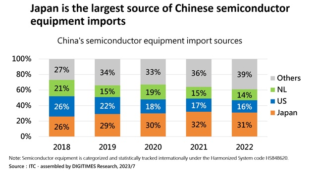
In 2022, according to Chen's research, over 60% of China's semiconductor equipment imports still came from the United States, Japan, and the Netherlands, with Japan remaining the largest source of semiconductor equipment for China, accounting for about 30% of import value.
Chen pointed out that nearly half of Japan's export controls are related to thin-film processing equipment. This category of equipment, however, involves a wide range of processes. In this context, export controls will primarily target products such as metal interconnect deposition equipment that employs materials like cobalt and ruthenium for advanced processes, atomic layer deposition (ALD) equipment used in sub-40nm processes, and hard mask deposition equipment required for multi-patterning processes.
Credit: DIGITIMES
Regarding lithography equipment, Chen believes that Japan's export of immersion deep ultraviolet (DUV) lithography equipment is likely to be impacted. Though Japan does not manufacture extreme ultraviolet (EUV) lithography equipment, Chen pointed out that the controls will nonetheless target EUV mask deposition equipment, equipment related to EUV process coating and development, as well as inspection equipment for blank or pre-exposed masks used in EUV equipment.
Notably, when it comes to etching equipment, Chen noted that Japan imposes restrictions on both wet etching and dry etching equipment for silicon-germanium (SiGe). In comparison, for other materials such as silicon, the control measures only touch on dry etching equipment. The analyst believes that Japan's stricter export controls on SiGe etching equipment are mainly driven by the widespread use of SiGe components in aerospace, military, and other industries.
About the Analyst
Eric Chen is an analyst and project manager at DIGITIMES Research. Chen received his Master's degree in international business from Taiwan's Soochow University. His research focuses on foundry industry as well as IC assembly & packaging industry.

Credit: DIGITIMES

