The era of AI is coming. It will not be long before our cities operate efficiently with tremendous amounts of devices and robots connected through 5G infrastructure with enough bandwidth for data handling and transferring. In order to analyze the huge amount of data coming from massive amount of edge devices (50B units by 2025), High Performance Computing (HPC) device is one of the key essential elements required for both end-terminals and also edge computing. Hence, the design and assembly of HPC chips is critical for semiconductor industry to address so that the bright AI enabled future for the society can be realized.
Heterogeneous integration: A back-end scaling approach to achieve more-than-Moore
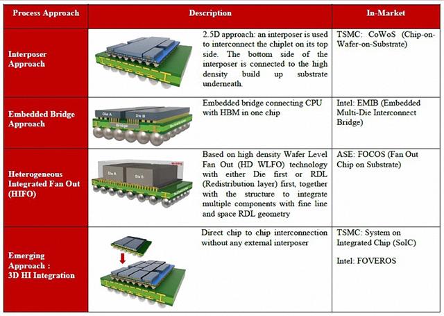
The Moore's Law has guided the semiconductor industry for many decades. However, it is approaching to the limit when the node size gets smaller than 14nm/10nm. Meanwhile, advanced node development has to be continued. To reduce the financial commitment for future node development, Heterogeneous Integration (HI) is the way forward. Switching from "only front-end node scaling" to "combination with back-end scaling," HI is a backend approach by means of advanced packaging technologies to integrate multiple chiplets, with different functionalities and each fabricated with best fit node in terms of technology and economic aspects, to reassemble an SoC (System on Chip) like function.
Impact of HI evolution to the supply chain
With the continued development of HI, we see significant impact on the supply chain for the industry. In the past, each player such as wafer foundry, OSAT and substrate supplier stays in his or her focus area. Nowadays, with HI, it opens up more business opportunities for each player by enlarging their served available market. Foundry is stepping into the advanced package assembly business; substrate house is also getting into the assembly process by offering passive and active embedding capability along with their substrate business. Although OSATs seem to be in a keen competition from both the foundry and substrate house, they are also pushing the development of more cost effective packaging technology to cope with the emerging but massive requirements of Edge and IoT devices required by the Al world. Without doubt, they will be facing many new technical challenges in the associated processes, critical material and enabling equipment.
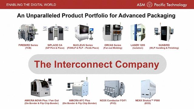
In order to shorten the development time in the advance packaging, working with a high-end equipment supplier - ASM Pacific Technology Ltd. can share their years-experience in R&D to overcome the challenges and save the cost. To build our AI future and enable the digital world, ASMPT will expect a greater collaboration and co-development work, together with different parties.
Please visit https://www.asmpacific.com/en/articles/ for full text.

There are different HI approaches currently and some are already in volume production mode

Impact of HI evolution to the supply chain
DIGITIMES' editorial team was not involved in the creation or production of this content. Companies looking to contribute commercial news or press releases are welcome to contact us.


