
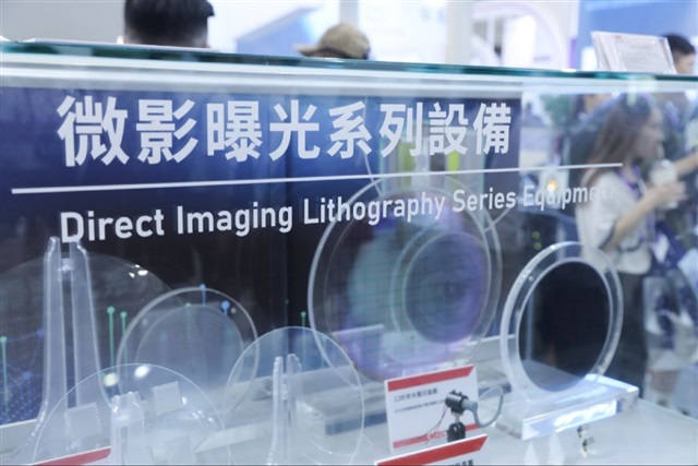
China's immersion DUV lithography programme has brought a little-known state-backed company into focus. Shanghai Aishengna Electronic Technology Group, founded in August 2023 with CNY7 billion (approx. US$1.03 billion) in registered capital, is reportedly coordinating limited production of domestically developed lithography systems.
Growing demand for AI chips is sending a larger share of South Korea's semiconductor exports to Taiwan, where Korean-made high-bandwidth memory (HBM) moves into advanced packaging processes led by TSMC.
Microsoft CEO Satya Nadella laid out how the company is scaling its AI infrastructure and platform to keep pace with demand. He outlined these plans during an earnings call on July 29, when he also announced record revenue above US$331 billion for fiscal year 2026 (ending on June 30), with Microsoft Cloud earnings surpassing US$214 billion and Azure earnings surpassing US$100 billion.
GlobalFoundries has signed a letter of intent with the US Department of Commerce for a potential US$300 million award to accelerate US development of silicon photonics technologies used in AI and high-performance computing data centres.
Memory prices are expected to remain elevated through 2026 as AI and data-center demand strains supply, with meaningful supply relief unlikely until well into 2027. A South Korean securities analyst argues that the squeeze could also make it harder for China to expand AI use, although Washington has not identified high memory prices as a policy tool.
Ennoconn Technologies held its 2026 Semiconductor x AI Applications Forum at Google's Asia-Pacific headquarters in Singapore on July 29 and signed a memorandum of understanding with the Singapore Manufacturers' Federation (SMF) on the same occasion. The event marked a further step in the Taiwanese technology group's expansion into Southeast Asia's semiconductor and artificial intelligence markets.
Samsung Electronics expects HBM4 sales to increase more than threefold sequentially in the third quarter of 2026, the company said on its earnings call. It projected that HBM4 will account for well over 60% of its total HBM revenue in the second half — a ramp that would lift its HBM market share broadly in line with its overall DRAM share and close the gap that has defined the HBM race since the AI boom began.