

Global Unichip Corp. (GUC), the Advanced ASIC Leader, announced today that the GLink-3D interface (GUC's Link for 3D die stacking) for the TSMC 3DFabric SoIC-X 3D stacking platform passed comprehensive silicon testing, validating 3DIC interface hardening flow. The first GUC 3D customer project also passed complete silicon testing, validating a full spectrum of 3D implementation services for AI/HPC/Networking applications.
Typical AI/HPC/Networking chips combine large memory with high performance logic. Logic gains power, speed and size improvement when scaled to the most advanced process while the SRAM scaling gains are moderate. Stacking a logic chiplet at a more advanced process node over an SRAM-dominant chiplet at a SRAM-scaling-efficient, less advanced node is the most optimal cost/performance solution. The high-bandwidth, low-latency, low-power GLink-3D interface IP is an enabler for this solution. Other challenges are thermal dissipation and power distribution of 3D stacked chiplets. GUC developed a full 3D design flow and implemented the first customer's logic-overmemory 3D stacking product and it passed silicon validation. A silicon-correlated design and simulation flow allows seamless implementation using the emerging UCIe-3D interface standard.
For the highest 3D interface bandwidth density requirements, GUC developed the GLink-3D interface using Double Data Rate (DDR) and adaptive timing architecture. The modular solution is flexible enough to support users' buses and clocking schemes and to avoid cross-die/corner timing closure challenge while providing 9 Tbps/mm2 bandwidth density. GLink-3D was validated using TSMC's first SoIC-X testchip with N5 CPU logic over N6 SRAM stacked dies. IP robustness was validated across a full range of process-voltage-temperature corners, proving BER <1E-30, high supply voltage and frequency margins, and strong supply noise immunity. The next generation GLink-3D for N2 to N7, targeting 20-40Tbps/mm2, 0.2ns-0.6ns latency and UCIe-3D compliant, is also under development.
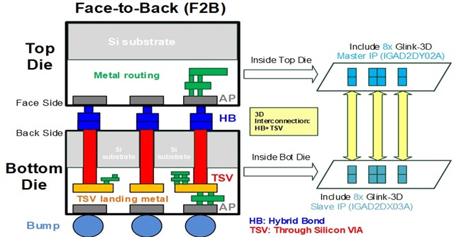
Multiple GLink-3D IPs were implemented in both dies of the SoIC-X testchip
"3D packaging moves chiplet interface from die edge to the most optimal location anywhere in a chiplet, making the shortest interconnect between logic and memory," said Aditya Raina, CMO of GUC. "Together with CoWoS®, InFO, and SoIC design expertise, package design, electrical and thermal simulations, and DFT and production testing, we provide our customers with a robust and comprehensive solution, enabling fast design cycles and quick time-to-market of their AI/HPC/xPU/Networking products."
"3D technology enables systems combining huge processing power and vast memory, with each component created in the most efficient process node," said Igor Elkanovich, CTO of GUC. "We developed and silicon-validated 3D interface (GLink-3D) hardening service, 3D physical implementation and timing closure, signal integrity, power distribution and integrity, and SoIC thermal and mechanical simulations – a full package of services allowing low risk adoption of 3D technology in our customers' projects."
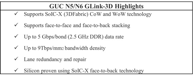
GUC N5/N6 GLink-3D Highlights
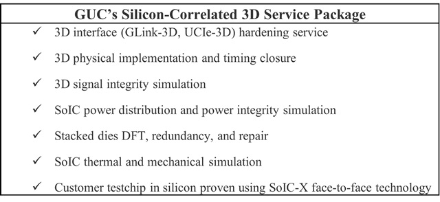
GUC's Silicon-Correlated 3D Service Package
Learn More about GUC's GLink IP with InFO/CoWoS Total Solution
For more information, please contact your GUC sales representative directly or email guc_sales@guc-asic.com
CoWoS® is a registered trademark of Taiwan Semiconductor Manufacturing Co. in the United States, Europe, China, Taiwan and/or other countries.