Global Unichip Corp. (GUC), the Advanced ASIC Leader, announced that GLink 2.3LL (GUC's die-to-die Link) interface IP for TSMC CoWoS and InFO chiplets integration platforms passed silicon validation and was showcased at the TSMC 2022 Open Innovation Platform (OIP) Ecosystem Forum in Santa Clara Convention Center on Oct 26, 2022.
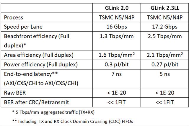
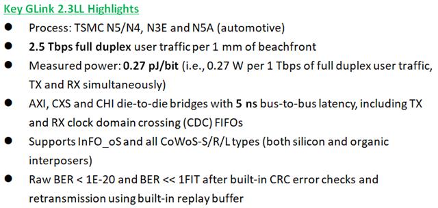
Die edge is the scarcest resource and GLink 2.3LL allows the most efficient use of it by transferring 2.5 Tbps of full-duplex user traffic per every mm of die edge. With end-to-end latency of 5 ns and measured power consumption of 0.27 pJ/bit, this is the most efficient chiplet interface on the market. GLink 2.3LL supports InFO_oS and all CoWoS types (both silicon –S and organic interposers -R). Leading AI, CPU, and automotive customers have adopted it for their next-generation products.

GLink 2.0 and GLink 2.3LL specifications
GUC provides full AXI, CXS or CHI bus bridges with configurable parameters (bus width and other properties) using a GLink 2.3LL physical interface. Integrated TX and RX Clock Domain Crossing (CDC) FIFOs allow independent clock frequencies for interconnecting dies, which can be changed on the fly without any data traffic interruption. The GLink 2.3LL IP includes a Link Training hardware state machine and automatic tracking of voltage-temperature changes during normal operation, so that the user software is not involved in interface control. The training and tracking are done entirely on the RX side without any die-to-die interaction, meeting strict Automotive Functional Safety requirements. The GLink 2.3LL I/Os' high cross-talk tolerance allows CoWoS/InFO unshielded routing, effectively doubling the number of signal traces for the interposer or RDL. GLink 2.3LL has redundant lanes that replace faulty ones during production tests or in the field. The proteanTecs interconnect monitoring system is integrated into the PHY. It can be used to monitor the signal quality of every physical lane during normal operation in order to observe lane degradation due to TSMC CoWoS or InFO_oS physical effects. This supports decisions to replace marginal quality lanes with redundant ones to prevent system failures and extend the product's life cycle.
The version of GLink 2.3LL for TSMC N3E will be available in Q1, 2023 and the GLink automotive version on TSMC N5A process will be ready in 2024. GUC's implementation of UCIe takes advantage of our expertise with many silicon-proven generations of GLink IPs, making our path to UCIe low risk.
"Chiplet-based architectures using CoWoS and InFO have become mainstream for infrastructure products and GUC is uniquely positioned with its long experience of developing HBM and GLink IPs and high-volume manufacturing CoWoS products. With the new GLink 2.3LL silicon validation, GUC demonstrates its long-term commitment to providing the most competitive 2.5D total solution, including a first-in-the-industry silicon-proven HBM3 PHY & Controller, GLink 2.5D and 3D chiplet interfaces, electrical and thermal simulations, package design, DFT and production tests, CoWoS and InFO manufacturing expertise," explains Sean Tai, president of GUC.
"We are designing our IPs for error-free operation in >1000W multi-chiplet ASICs. We test their immunity to high power noise, temperature and voltage cycling, with months of error-free operation in very harsh conditions. We leverage our ASIC production experience to define a comprehensive silicon validation test suite. We are committed to doubling bandwidth density every year while keeping power and latency low, enabling the CPU, GPU, DPU, AI, automotive and network processors of the future," said Igor Elkanovich, CTO of GUC.

Key GLink 2.3LL highlights
Learn More about GUC's GLink IP with InFO/CoWoS Total Solution
For more information, please contact your GUC sales representative directly or email guc_sales@guc-asic.com