In a strategic move to bolster India's semiconductor sector, Sahasra Semiconductors, a nascent player in the chip-making segment, has unveiled plans to commence assembly, testing, marking, and packaging (ATMP) production.
The company will initially focus on basic packaging, identified as 'low-hanging fruit,' which are presently being imported from China. This initiative not only marks Sahasra's foray into the burgeoning semiconductor market but also signals a step towards reducing dependency on Chinese imports in the domain.
"In several domains where our design activities are underway, we observe a significant gap, with minimal activity from other entities and a dominant influx of products from China," explained Varun Manwani, CEO of Sahasra Semiconductors. "When it comes to lower-end packages, China is the predominant supplier. While high-end packages might originate from various countries and notable brands, the market for smaller or basic packages is essentially monopolized by China. Given India's and the global market's pivot, a substantial opportunity has unfolded. The extent and nature of what we can achieve within this window of opportunity remain exploratory, yet the potential is undeniably vast."
Background
Having been in operation for the last 23 years, the organization has primarily functioned within the electronics hardware manufacturing space. The venture into the solid-state memory business came in 2016, marking the beginning of a collaboration with the global giant, Sony.
However, this partnership was short-lived, enduring only two and a half years, due to Sony's decision to withdraw from the memory business worldwide in 2018. The relationship concluded around early 2019. Nonetheless, during their alliance, the seeds for exploring packaging were sown, spurred by the peak valuations being achieved in India at the time.
"Even though they pulled out of this market, we decided to continue exploring the possibility," Manwani said. "For about a year or so, we were trying to finalize plans, now that Sony was no longer available as a customer. However, we were quite determined that this was the right direction. In 2020, after the pandemic started, the government introduced the entire PLI scheme, which gave us a push to look at this seriously and try to take advantage of the opportunity. Simultaneously, the entire shift, including the US-China trade war, was an impetus in the sense that we could see the writing on the wall: in the next few years, there would be a lot of manufacturing and demand out of India."
From memory to beyond
Initially, the company contemplated a sole focus on the memory business, leveraging an existing market in memory products with the assumption that managing the packaging of memory solutions would naturally cater to that market. However, given the substantial shift in the memory business market, particularly with no entities engaging in any form of packaging in India, and being one of the pioneers in this domain, the company did not immediately embark on high-level or advanced packaging. Instead, a strategic decision was made to commence with what can be described as low-end or low-hanging fruit, such as UDPs, utilized in USBs, or microSD cards, which find applications in various devices.
"As I mentioned, the market shift that occurred from a 2016 standpoint to 2020, where all smartphones became much more popular and came with internal memory, caused the overall volume of microSD cards to drop considerably worldwide and in the Indian market," Manwani said. "Having said that, we still started with microSD and UDPs because that is the low-hanging fruit, and by being able to do that, it's a learning exercise for us. So, it actually aligns with our roadmap, and we are ready to go into the higher-end packages of eMMCs, USFS, and UDFs. This is the right steppingstone towards getting into those packages."
Investment
In the initial phase of its development, the company has allocated a $20 million investment. To date, $15 million of this sum has already been invested, with the remaining $5 million currently in the process of being allocated for additional orders with vendors, among other expenses, yet is firmly committed as part of phase one.
Moving forward into phase two, the company plans to inject an additional $30 million, bringing the total investment for both phases to $50 million. As the business grows, further scaling up will be necessary, involving the addition of more equipment at various stages to address potential bottlenecks, typically in areas such as wire bonding and die bonding, to facilitate subsequent scale-up.

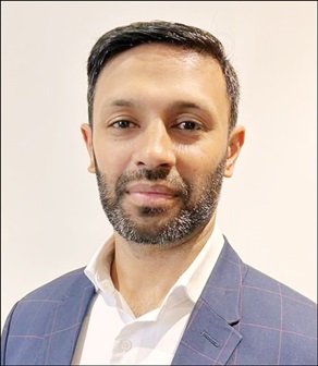
Varun Manwani, CEO, Sahasra Semiconductors. Credit: Sahasra.


