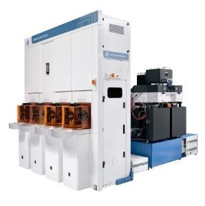
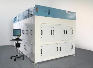
Applied Producer InVia dielectric deposition system
Applied Materials has added to its line of 3D chip packaging solutions with the launch of...
Photo: Company
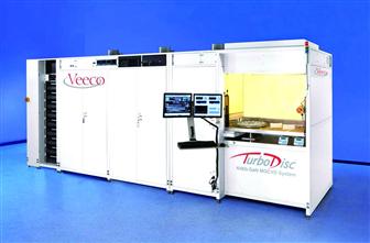
Veeco TurboDisc K465i GaN MOCVD system
Veeco Instruments has introduced a new gallium nitride (GaN) MOCVD system for production...
Photo: Company
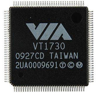
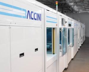
VIA Vinyl EnvyUSB 2.0 audio controller
VIA Technologies has unveiled the VIA Vinyl Envy VT1730 USB 2.0 audio controller. The VIA...
Photo: Company
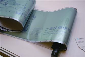
ITRI laser technology for flexible electronics applications
Industrial Technology Research Institute (ITRI) has developed a new laser technology for...
Photo: CJ Liu, Digitimes
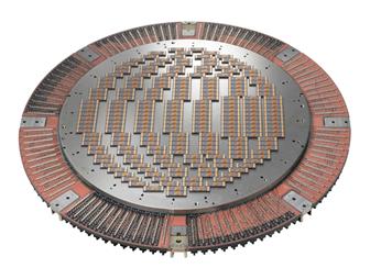
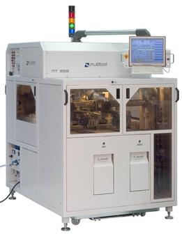
FormFactor 300mm full-wafer test solution for DRAM
FormFactor has introduced its next-generation 300mm (12-inch) full-wafer-contact probe card...
Photo: Company
Applied Reflexion GT
Applied Materials has launched its Applied Reflexion GT system for advanced metal CMP applications...
Photo: Company
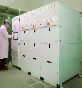
Applied iSYS
Applied Materials has unveiled what it claims is the industry's first fully-integrated abatement...
Photo: Company
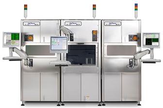
KLA-Tencor ICOS WI-2250
KLA-Tencor has introduced its ICOS WI-2250 wafer inspector for MEMs and LED manufacturing...
Photo: Company

Applied Materials Solar Technology Center in China
Applied Materials has opened an advanced solar research and demonstration facility in Xian,...
Photo: Company
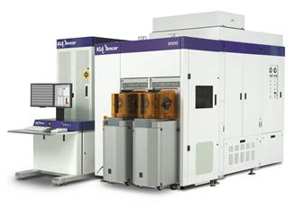
KLA-Tencor 8900 inspection system
KLA-Tencor has extended its product offerings in the CMOS image sensor (CIS) market by announcing...
Photo: Company
Applied HCT Diamond Squarer for solar wafers
Applied Materials has introduced ts new HCT Diamond Squarer system, which can reduce the...
Photo: Company
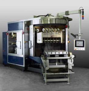
Multitest automatic contactor cleaning feature
Multitest Elektronische Systeme, a manufacturer of test equipment for semiconductor, has...
Photo: Company

Applied Topmet 4450 system
Applied Materials' new Topmet 4450 system deposits ultra-thin aluminum films on 4.5m wide...
Photo: Company
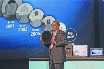
IDF San Francisco: Intel CEO displayed a silicon wafer built on 22nm process
Intel president and CEO Paul Otellini has displayed a silicon wafer containing its first...
Photo: Monica Chen
Applied Materials multiple printing technology for solar cells
Applied Materials has announced its Baccini Esatto technology, a multi-step screen printing...
Photo: Company