According to market research reports, the global wafer foundry market size was about US$82 billion in 2020, with TSMC having a 55% global market share, and Samsung taking only 15%. In terms of profit in the global wafer foundry sector, TSMC took nearly 85%, compared with less than 5% for Samsung. In other words, TSMC's profit in wafer foundry business was 17 times Samsung's. Evidently, the two players are competing in different divisions. But why has Samsung been so constantly provocative? Why is South Korea going all-out, vowing to be a dominant power in the global semiconductor industry by 2030?
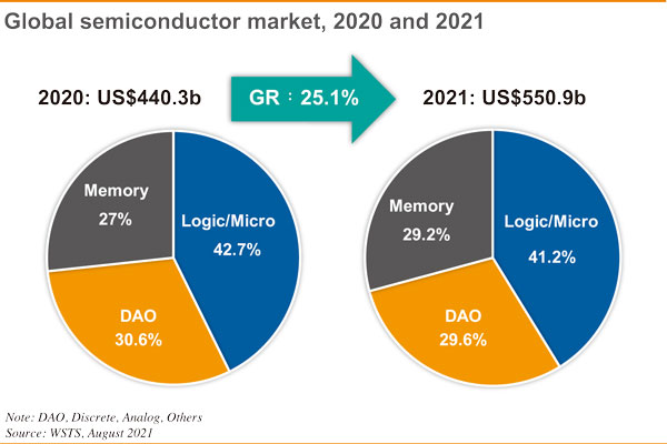
According to statistics of WSTS, the global semiconductor market size was US$440.3 billion in 2020, and is expected to grow by 25.1% to US$550.9 billion in 2021 - the first time that the global semiconductor market will exceed the US$500 billion mark. The memory sector will reach US$161.11 billion in 2021, up 37.1% from 2020. This is good news for Samsung, which has a 40% global market share. It is also crucial to Korea's semiconductor industry in 2021.
Of Samsung's revenue in 2020, 30.8% was contributed by semiconductors, which accounted for 52.2% of its profit. It is estimated more than 55% of its 2021 revenue will be from semiconductors. Above all, more than 90% of the profit of the entire semiconductor division come from its memory business. For Samsung or South Korea as a whole, the semiconductor industry structure is too much tilting towards the memory sector, which is a big concern of South Korea. It is generally believed that logic chips and microprocessors offer diversity that can diversify risks and create high value-added business opportunities - an advantage that is lacking in the memory sector. TSMC may have already built a high barrier, but South Korea is hardly ready to concede defeat, still hoping to take over the market leadership.
What are the possible scenarios where Samsung could surpass TSMC? In general, we can analyze the competitive advantages and disadvantages of wafer foundry from node process technology, ecosystem and customer structure. Up to 28nm, the evolution of node process technology had been mostly materials-driven, such as copper interconnect process, low dielectric insulators, etc. Not until 14nm node process did the driving force come from structural innovation. The Samsung-developed FD-SOI process was different from TSMC's FinFET. The arrival of 7nm has brought pressure from both materials and structure innovation. Structurally, the new era of GAAFTE requires materials innovations including the application of new materials such as boron nitride (hBN) and transition metal disulfur compounds (TMD). According to the timeline disclosed by Samsung, Samsung will overtake TSMC in GAAFTE. But Samsung often has seen delays in its projects, so the timeline may not mean much, unless you can really secure orders from top-notch customers with advanced node process.
To surpass TSMC, Samsung, in addition to process technology refinement, will have to address issues such as equipment investment, customer support and ecosystem practices. Of course, the competition in the world's hot markets is by no means a game play. A customer's orders often worth billions of dollars have set everyone's nerves on edge. Taiwan and South Korea have their owns advantages. Let us keep an eye on the race.

(Editor's note: This is part of a seies of analysis by DIGITIMES Asia president Colley Hwang, focusing on Samsung with comparisions of the IT industry developments in Taiwan, South Korea and China.)


